01
High-Speed Production
Semiconductor wafer polishing (Chemical Mechanical Planarization – CMP) lines operate at high speeds, necessitating rapid and precise inspections.
02
Defect Detection
Identifying surface defects such as scratches, pits, and uneven polishing that can affect subsequent processing and device performance.
03
Consistency and Quality
Ensuring each polished wafer meets stringent surface quality and flatness requirements.
04
Efficiency Requirements
Reducing downtime and maintaining high production speeds without compromising quality.
StroboX Solution
Key Features and Integration Potential
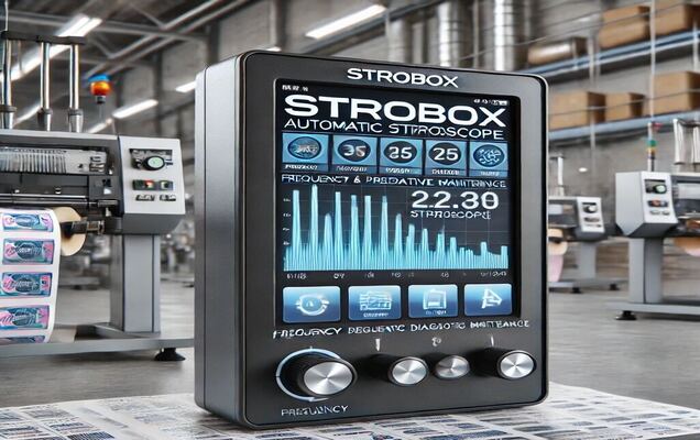
- Automated Speed Detection: Measures polishing line speed and adjusts the strobe effect to match, ensuring precise imaging at high speeds.
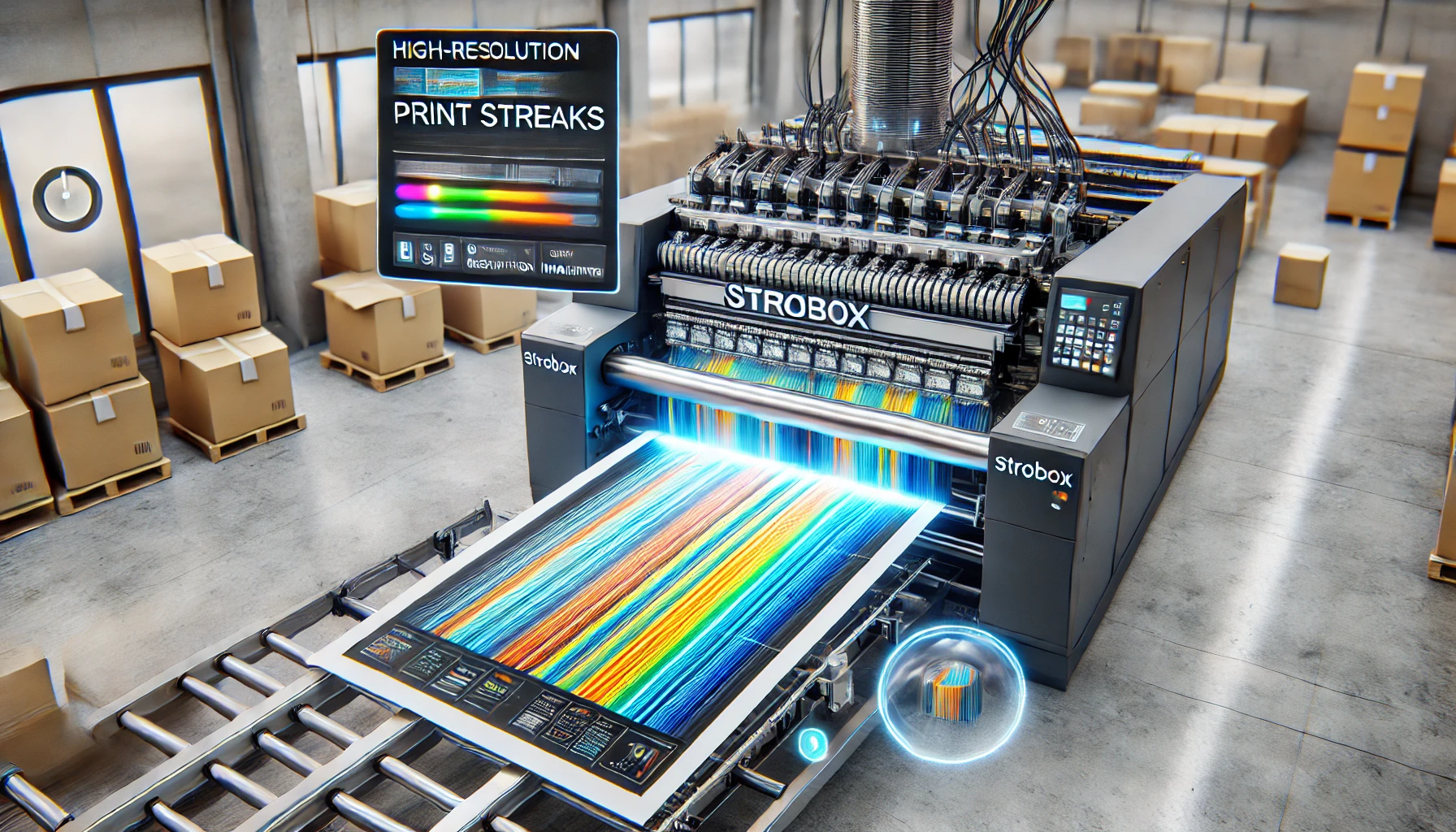
- High-Resolution Imaging: Captures detailed images of polished wafer surfaces, identifying even the smallest defects.
- AI-Powered Analysis: Compares images to standard quality benchmarks to accurately identify and classify defects.
- Instant Alerts: Provides immediate notifications for detected defects, enabling quick corrective actions.
- Integration with Manufacturing Systems: Integrates seamlessly with existing semiconductor polishing and quality control systems, ensuring streamlined workflows and minimal disruption.
Usecases

Feature: High-Resolution Imaging
Benefit: Detects surface defects such as scratches, pits, and micro-scratches in real-time, ensuring high-quality polished wafers.
Feature: AI-Powered Analysis
Benefit: Ensures the uniformity and flatness of the wafer surface, enhancing the reliability of subsequent lithography and etching processes.

Potential Benefits
01
Increased Efficiency
Automates the inspection process, significantly reducing the need for manual inspections and associated labor costs.
02
Enhanced Accuracy
Provides precise and consistent quality checks, minimizing the risk of defective wafers proceeding to subsequent manufacturing steps.
03
Higher Yield
Improves yield rates by detecting and addressing defects early in the polishing process.
04
Cost Savings
Reduces rework and scrap rates, leading to substantial cost savings.
Challenges and Considerations
- Technical Complexity: Ensuring the system can handle various wafer materials, sizes, and polishing processes.
- Quality Assurance: Maintaining high standards in automated defect detection and classification.
- Integration Challenges: Integrating seamlessly with existing polishing and quality control systems.
- Scalability: Ensuring the solution can scale to meet the demands of large-scale semiconductor fabs.